Noise in Switched Capacitor Circuits
I’ve previously covered the topic of noise in circuits and figured I’d elaborate even further. Many ICs use some sort of switched-capacitor circuit for SOME reason (sample-and-hold, for example) and the noise associated with such a circuit is not as straight-forward as you would initially assume. A lot of engineers will just approximate the noise variance of a sample-and-hold circuit as $ \frac{kT}{C} $ which is a bad assumption in most cases. In fact, it’s so commonly overlooked that Richard Schreier (of Analog Devices fame) wrote a great paper on this very subject [1].
So how can we determine the noise of the above circuit? Well, you do the same thing you’d do with any other circuit: math. To get the RMS noise of any circuit you need the noise transfer function. To get the noise transfer function (NTF) of a circuit who’s signal transfer function (STF) is $\lvert H(s)\rvert $ you have to integrate the square of the STF such that:
| ++ NTF = \int_{0}^{\infty} | H(2\pi f) | ^2 df ++ |
After deriving the NTF, the RMS noise is given by multiplying the PSD of the noise and dividing by the square of the closed-loop gain (which is ‘1’ for a unity gain buffer). Therefore:
++ v_{n}^2 = \frac{S_{vo}}{A_{CL}^2}\int_{0}^{\infty}\lvert H(2\pi f)\rvert ^2 df ++
Neat. Now what?
Well, first you need to recognize that the closed-loop output impedance of a unity gain buffer is roughly given by $ \frac{1}{G_M}$ where $ G_M$ is the trans-conductance of the amplifier whose DC open-loop gain transfer function approximates to $ G_MR_{out}$. Also, since we are only interested in what the noise looks like right before the switch opens (ie. we just took a sample), we can approximate the switch as an effective resistance $ R_{SW}$. So now we have two resistors, each with independent noise sources, and one capacitor, as shown in the equivalent small-signal model below. From here, it’s just a matter of solving each circuit with only one of the independent noise sources active and then summing the ensuing expressions.
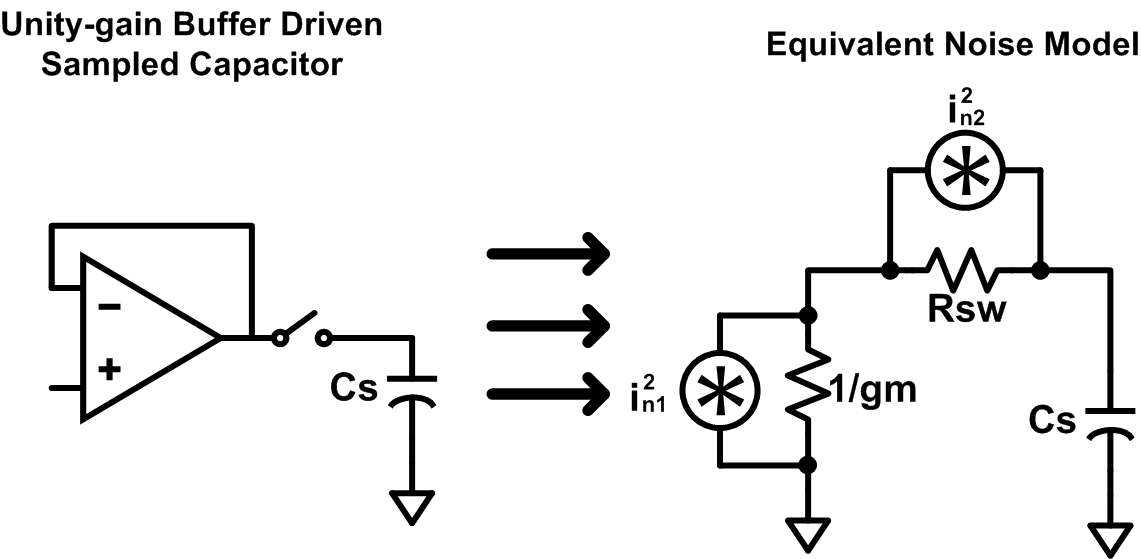
The first noise source, $ i_{n1}^2$, is the equivalent output noise current of the amplifier. You can also use the equivalent output noise voltage by putting the noise source in series with the resistor, rather than in parallel. After removing the noise source associated with the switch resistance (and setting the positive plate of the capacitor as out output node), we can generate a transfer function in the Laplace domain of:
++ V_O = V_N \frac{1}{sC_S(R_{SW}+\frac{1}{G_M})+1} ++
Using the method described earlier, we can easily figure out the RMS noise due to the amplifier. As Schreier shows in his paper (which can also be easily derived), for a single-pole low-pass transfer function $ \frac{G_0}{s\tau+1} $, the noise variance is given as:
++ \overline{v_{n}^2} = \frac{G_0^2S_{V}}{4\tau} ++
The time constant for the amplifier’s noise source is $ C_S(R_{SW}+\frac{1}{G_M})$ and the power spectral density depends on the specific amplifier implementation; however, we can assume that the PSD can be approximated as $ S_{V,amp} = \frac{4kT\gamma_{eff}}{G_M}$ where $ \gamma_{eff} $ contains two components: a process-driven parameter $ \gamma$ and some multiplicative factor that accounts for other noise sources in the amplifier. Plugging all of this in yields:
++ \overline{v_{no,amp}^2} = \frac{kT}{C_S}\frac{\gamma}{G_MR_{SW}+1}++
Next, we need to analyze the circuit with the amplifier’s noise source removed and with the switch noise source only. The ensuing Laplace-domain transfer function is:
++ V_O = V_N \frac{1}{sC_SR_{SW}(1+\frac{1}{G_MR_{SW}})+1}++
Using the same method as before, the noise variance at the capacitor due to the switch is:
++ \overline{v_{no,sw}^2} = \frac{kT}{C_S}\frac{G_MR_{SW}}{G_MR_{SW}+1}++
Since these noise sources are uncorrelated, we can just sum the variances due to each component to get the total noise variance of the circuit:
++ \overline{v_{no}^2} = \frac{kT}{C_S}\frac{\gamma+G_MR_{SW}}{G_MR_{SW}+1}++
Clearly, this noise variance is not simply $ \frac{kT}{C}$ (which is unfortunate), and depends on other circuit parameters. So, how much of a problem is this? Here’s an example: say we have a unity-gain buffer with an effective trans-conductance of $ 200\mu S$, a switch resistance of $ 1k \Omega$, and a capacitor of $ 1 pF$. Oh, and we’re operating at room temperature and let’s use $ \gamma_{eff}=\frac{4}{3}$. If we assume $ \frac{kT}{C}$ noise, the RMS output noise would be around $ 64 \mu V$. However, using the more accurate equation we derived, this RMS output noise is actually closer to $ 82 \mu V$. So, how can we avoid this issue (without blowing up the capacitor size…) Well, $ \gamma$ is a fixed, process-driven parameter, but we can play with the multiplicative factor in the $ \gamma_{eff}$ term by designing our amplifier such that the input pair’s noise dominates and all other sources are negligible. The closer to 1 that you can make $ \gamma_{eff}$, the better (because then the numerator and denominator cancel- yay!). An interesting thing to note is that as you start to decrease the switch resistance down to $ 0 \Omega$, the effective RMS output noise becomes
++ \overline{v_{no}^2} = \gamma_{eff}\frac{kT}{C_S}++
So, moral of the story: design a great amplifier if you care about noise in a switched system. You can’t argue with math.
References
[1] Richard Schreier et al., “Design-Oriented Estimation of Thermal Noise in Switched-Capacitor Circuits” in IEEE Transactions on Circuits and Systems-I: Regular Papers, vol. 52, no. 11, pp. 2358-2368, Nov. 2005.