Inversion Coefficient Based Circuit Design
One of the forums I attended this year at ISSCC 2016 was entitled “Advanced IC Design for Ultra Low-Noise Sensing”. There were a variety of great speakers, but the presentation given by Professor Willy Sansen was particularly interesting because it introduced me to a design methodology I was not familiar with: designing via the “inversion coefficient” of a MOSFET.
What is an Inversion Coefficient?
The concept of the inversion coefficient comes from a unified all-region MOSFET model known as the “EKV Model” which was named for the creators: Enz, Krummenacher, and Vittoz [1]. This inversion coefficient simply defines which operating region the MOST is in and how deeply it’s in this region. As a rule-of-thumb: as this “inversion coefficient” number increases above ~10, the device operates deeper in strong inversion and as the number decreases below ~0.1, the device operated deeper in weak inversion. So how is this inversion coefficient defined? Well, it’s the expression for drain current divided by some normalization current (which [1] calls the “specific current”). This normalization current is defined as $I_S = 2\beta \phi_{t}^{2} $ where $\phi_t$ is simply the thermal voltage $\frac{kT}{q}$. Once this ratio is taken, the inversion coefficient is defined as:
++i_f = \frac{I_D}{I_S} = \left[ln\left(1+exp\left(\frac{V_{GS}-V_{TH}}{2n\phi_t}\right)\right)\right]^2++
What this equation says is exactly what we would expect: the operation region of a MOST is determined by its biasing conditions. The interesting part is that now we can potentially choose where we’d want the transistor to operate (weak/moderate/strong inversion) and figure out the required drain current and voltage biasing required… but first, we need a few more equations to begin to do any sort of design, primarily an expression for the trans-conductance as a function of the inversion coefficient.
Dr. Sansen actually derives this expression in his book, “Analog Design Essentials” [2], where he shows that a MOST’s trans-conductance is:
++ g_m = \frac{I_D}{n\phi_t}\cdot\frac{1-exp\left(-\sqrt{i_f}\right)}{\sqrt{i_f}}++
This equation is interesting because it claims that for a constant current, you can modify $g_m$ just by changing the region that the MOST operates in (ie. change $V_{GS}$).
Similar to the EKV model, Cunha _et. al_published a paper in 1998 where she derived the cutoff-frequency for a MOST in terms of the inversion coefficient [3]. This is defined below:
++f_t = \frac{\mu\phi_t}{2\pi L^2}\cdot 2\left(\sqrt{1+i_f}-1\right) ++
Again, we see an interesting relationship that indicates we can control the fundamental speed-limit of a MOST by simply modifying its region of operation (as well as length) but we don’t have to change the power consumption.
So how could we utilize the inversion coefficient idea to optimize a design for speed, noise, and power? Well, in Sansen’s presentation at ISSCC, he made the following assumptions to illustrate how to optimally design for those three parameters:
- Noise will usually be dominated by contributions from $\frac{kT}{C}$
- The GBW of a circuit is some form of $\frac{g_m}{2\pi C}$
- We can re-write $g_m$ as $2\pi\cdot GBW\cdot C$ which allows us to keep the trans-conductance constant for a constant noise (C) and a constant speed (GBW)
Design Using the Inversion Coefficient
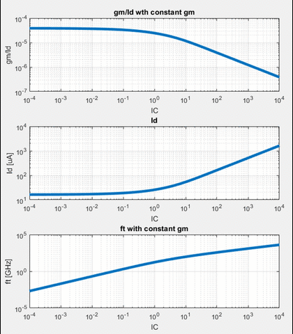
Given the assumptions laid above, we can plot $\frac{g_m}{I_D}$, $I_D$ and $f_t$ all as a function of the inversion coefficient for a constant $g_m$. In the animated image below, you can see the following trends:
- As we go deeper into strong inversion, we lose $\frac{g_m}{I_D}$ efficiency.
- As we go deeper into weak inversion, we lose speed for no power beneift
- We can optimize for speed or power by keeping the device operating in moderate inversion
Sansen’s rule: an inversion coefficient of ‘1’ is typically the most optimal point for speed, noise, and power.
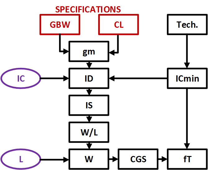
In the Fall 2015 edition of “IEEE Solid-State Circuits Magazine”, Sansen published the following flowchart, illustrating a design flow using the inversion coefficient where the designer only needs to make two choices: the actual inversion coefficient, and the length of the device [4]. All other parameters will fall out of the equations.
Let’s do a little exercise to see this methodology work. Say we are asked to design a simple 5T OTA with a required DC Gain of 40dB, GBW of 100 MHz and a load capacitance of 1 pF.
- Calculate $g_m$
- Here we can use $g_m=2\pi\cdot GBW\cdot C_L$ which gives us $g_m\approx 630 \mu S$
- Choose $i_f$ and calculate required drain current
- Let’s use $i_f=1$. Remember, this is our first of two design choices!
- Now we can plug this into $ g_m = \frac{I_D}{n\phi_t}\cdot\frac{1-exp\left(-\sqrt{i_f}\right)}{\sqrt{i_f}}$ and solve for $I_D$ which ends up being $I_D\approx 0.001\cdot n\phi_t$. The parameter ‘n’ is process-dependent, but let’s assume it’s equal to ‘1’ and solve this at room temperature which yields $I_D\approx 26 \mu A$
- Using our drain current value, we can calculate $I_S = \frac{I_D}{i_f} = 26 \mu A$
- Next, we need to know $\mu C_{ox}$ for our process in order to extract the required $\frac{W}{L}$ ratio.
- Let’s just say $\mu C_{ox} = 100 \mu A/V^2$
- Given this and the fact that $I_S = 2\mu C_{ox}\frac{W}{L}\phi_{t}^{2}$, we can solve for the width-to-length ratio which results in $\frac{W}{L}\approx 194$
- Now we get to make our last design choice: length. The length is going to end up determining our non-dominant pole frequency, as well as our DC gain (since it will impact the output resistance). Let’s choose $L=0.5 \mu m$
- This results in $W=97 \mu m$
- The cutoff frequency can be found via $f_t = \frac{\mu\phi_t}{2\pi L^2}\cdot 2\left(\sqrt{1+i_f}-1\right) $ which indicates that $f_t \approx 55 GHz$ for $ \mu \approx 400 \frac{cm}{V\cdot s}$
So our final list of design parameters for the input pair of our 5T OTA is:
- $I_D = 26 \mu A$
- $\frac{W}{L} = \frac{97 \mu m}{0.5 \mu m}$
- $g_m = 630 \mu S$
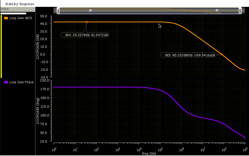
I went ahead and put a schematic in cadence using a PDK I have access to and got the following result using stability analysis. We hit our desired 40dB gain target and are quite close to the GBW requirement of 100 MHz (it turns out, the trans-conductance is a bit low in the simulation due to a mismatch between the actual transistor $\mu C_{ox}$ and what we used as an approximation).
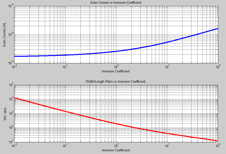
Instead of haphazardly choosing the inversion coefficient, we could also sweep this value to try and find an optimum point for our application. Below is a plot of the drain current and width-to-length ratio versus a sweep of the inversion coefficient. Using a plot like this would allow for an optimization of area and power given the GBW and load capacitance requirements.
Conclusion
Hopefully I’ve shown the power of using the inversion coefficient as a basis for design. Being able to quickly, and intelligently, optimize for power/speed/noise/area/etc. is extremely important and the inversion coefficient method that Sansen presented in the forum at ISSCC this year is quite ideal for this.
References
[1] Enz et. al, “An Analytical MOS Transistor Model Valid in all Regions of Operation and Dedicated to Low Voltage and Low Current Applications”, in Analog Integrated Circuits and Signal Processing, 1995.
[2] Sansen, “Analog Design Essentials”, Springer 2006.
[3] Cunha et. al, “A MOS Transistor Model For Analog Circuit Design”, in Journal of Solid State Circuits, 1998. [4] Sansen, “Minimum Power in Analog Amplifying Blocks”, in IEEE Solid-State Circuits Magazine, 2015 (vol. 7, issue 4)