My Circuit Design Methodology
I’ve gotten a lot of feedback regarding my post last year outlining design using the Inversion Coefficient and figured it was time to outline how I go about designing a given circuit. If you haven’t read through my first post, I’d recommend it to get a handle on why use of the Inversion Coefficient is so powerful. Before I begin, I want to summarize my method here. I am using a dual approach: gm/Id methodology wherein I characterize a device and create a lookup table to choose device characteristics, as advocated by Dr. Boris Murmann, as well as the inversion coefficient method advocated by Dr. David Binkley and Dr. Willy Sansen.
Step 1: Characterize a Device
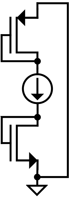
This step only needs to be performed once at the beginning of a project for a new PDK. Basically, you just want to characterize a given device’s current density requirement for a given gm/Id. First, we need to think about why we want to graph this (ie. what information will we gain?). If we can normalize the bias current of the device to the device’s W/L ratio, we should be able to sweep this parameter $\frac{I_D}{\square}$ which contains information on both the bias current and size of the device. Now, once we sweep this, we can plot two items: gm/Id and some figure of merit to determine the best bandwidth, which we will define as $A_0\cdot GBW$. In this method, one of either width or length will be a variable, so you can plot a family of curves for multiple lengths (or widths) and find any trends. The testbench to generate these results is very simple (see below). Here we are forcing a current through both a PMOS and NMOS device which are diode connected to maintain saturation. Most models I’ve ever worked with allows you to extract $\frac{g_m}{I_d}$ directly from simulation, so that’s easy. The next value we need is our FoM, which will just be: $\frac{g_m}{g_{ds}}\cdot \frac{g_m}{2\pi c_{gg}}$ where $c_{gg}$ is the total gate capacitance (typically available to extract in simulations).
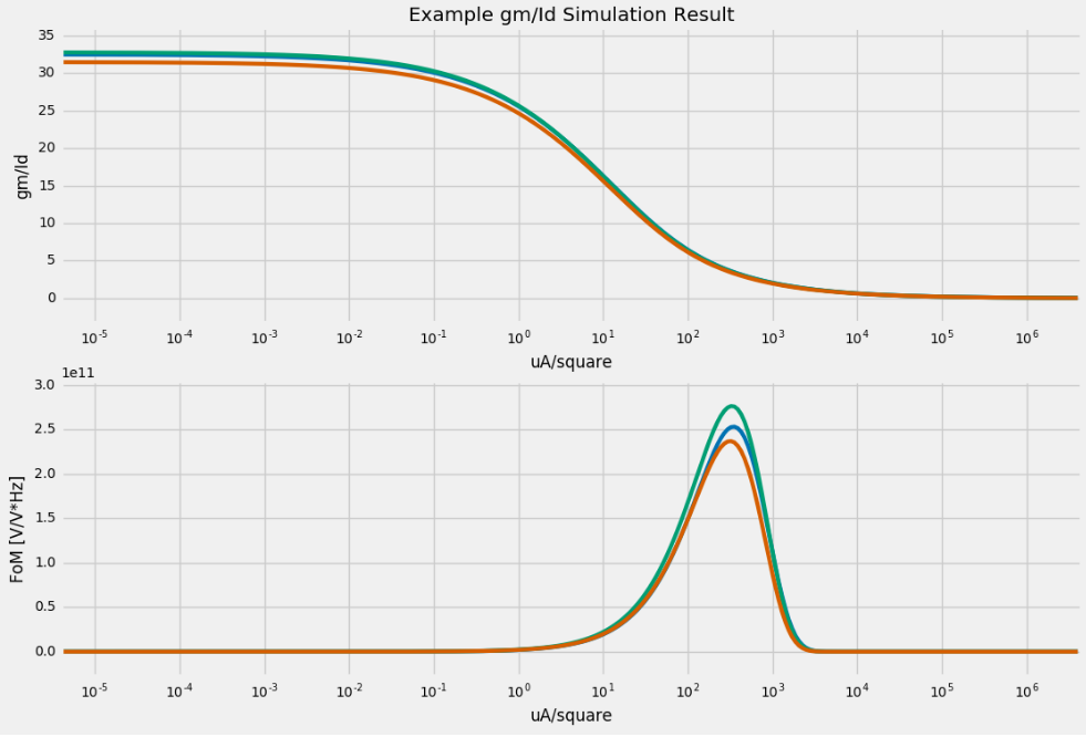
Below is an example output (I fudged numbers to create the plot so as to not disclose any process information from the PDKs I have access to). Here I have three lines corresponding to three different devices sizes (width or length, irrelevant for this example) and I plot $\frac{g_m}{I_D}$ as well as the FoM defined earlier.
Step 2: Create a Design Table
Now I’m done. I have characterized my device and never need to run this testbench again (as long as the PDK doesn’t drastically change). You can also run this over temperature and process corners and select a value based on your worst expected corner if you want. So from this, what I do (actually, it’s something my co-worker started to do that I adopted as well) is to create a simple table for a given $\frac{g_m}{I_d}$ and its corresponding current density. I choose three values: one to represent weak-inversion, one for moderate,and another for strong. For strong, I pick the value where the $\frac{g_m}{I_d}$ starts to curve; the above example is at roughly $\frac{0.1\mu A}{square}$. The next for moderate will be the middle of the two ‘knees’ on the curve and for strong I choose roughly where the FoM peak occurs. All of these points also correspond the what Dr. Sansen outlines as efficient operating points for power (weak inversion), speed (strong inversion) and an trade-off between speed and power (moderate). All of this information can be found in my previous post. Thus, I end up with the following table:
| $\frac{g_m}{I_d}$ | $\frac{\mu A}{\square}$ |
|---|---|
| 30 | 0.1 |
| 15 | 10.0 |
| 5 | 50 |
From this, we can relate $\frac{g_m}{I_d}$ to the inversion coefficient via the following equation: $ \frac{g_m}{I_d} = \frac{1}{n\phi_t}\frac{1-exp(-\sqrt{IC})}{\sqrt{IC}} $ With this, we can have a rule of thumb that a large $\frac{g_m}{I_d}$ means the device is in weak inversion, a small $\frac{g_m}{I_d}$ means the device is in strong inversion, and something in between is in moderate. We never have to break that equation out again so long as we remember it (however, it comes in handy for more complicated design exercises. For example, using the spectral voltage noise density equation in Dr. Binkley’s book in order to bound the acceptable values for IC. We can then back-calculate $\frac{g_m}{I_d}$ and find our required current-density that way).
Step 3: Choose $\frac{g_m}{I_d}$ Based on Design Specifications
Information in hand, we can proceed to sizing a device. The intuition for where to operate a device can come from a graph that I have modified and reproduced from Dr. Binkley’s MIXDES Conference paper here:
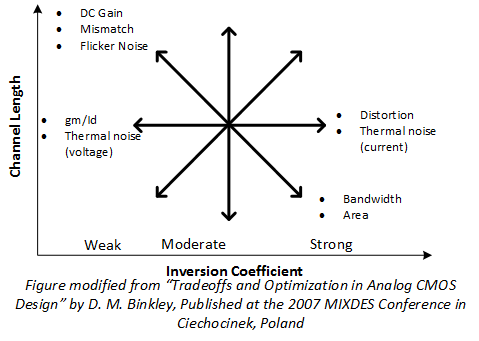
So, for example, say we have a differential input pair for an amplifier we need to size. The things we will care about (for pretty much any amp design) is to minimize mismatch, maximize gain, minimize thermal noise, and maximize bandwidth. Clearly gain and bandwidth directly oppose eachother on this graph: so how to we select our desired operating region? Here I come back to Dr. Sansen’s statement (please see previous post) about operating with an inversion coefficient of ‘1’ is about optimal for most applications: ie. operate in moderate inversion. Depending on our needs, we can always optimize the device further, but this will provide a very good and efficient starting point for our design (which is the whole point of this methodology). So, we look up the required current-density for a $\frac{g_m}{I_d}$ value that will place us in moderate inversion: in my example, this is $10 \frac{\mu A}{\square}$. We have two more requirements: to know our drain current and to know our length. Given that the device is an input pair, we probably don’t want too long of a length since it will increase our area by a lot (though, we do get an improvement in output impedance!) so let’s say it’s $1 \mu m$. Again, the beauty of this methodology is the fact that this will be a good optimal starting point and we can change it later while still maintaining our desired operating region. For drain current, it really depends on the application as well as current references readily available by the circuit. Let’s say it’s $100 \mu A$ because we need to reduce the noise of our circuit and have a relaxed power budget. Given this, we can calculate our require W/L ratio as: $\frac{W}{L} = \frac{100 \mu A}{10 \frac{\mu A}{\square}} = 10 \frac{\mu m}{\mu m} $ Given we chose a length of $1 \mu m$, our width is then $10 \mu m$. Done!
Conclusion
I know some of my statements seem wishy-washy (choice of drain current, for example). The thing is, most of this information is tightly bound in a real design: we have noise targets, the circuit has to fit in a certain area, the circuit can only consume so much power, we have to operate at a certain frequency, etc. This is part of a design: there’s no one-size-fits-all solution. What we can do, however, is use Dr. Binkley’s graph to choose a good starting point for our design. This method is very efficient at approximating an optimal design, allowing you to arrive at an optimal design much more quickly than traditional methods (while drastically limiting the number of calculations you need to perform). It also, crucially, helps to eliminate the trap many designers can fall into where they parameterize their circuits to all hell and run hundreds of simulations to find an optimal point. This is terrible as it never allows a designer to truly understand their circuit (just like using only square-law equations gives you very little insight into a circuits true operation). Dr. Binkley’s graph is great because it allows a designer to familiarize themselves with the correlation between a device’s operating region and common circuit specifications. In addition to this, it allows for a designer to intelligently tweak their design by modifying the operating region for a desired result which means the designer will be forced to know exactly why each device is sized and biased the way it is (whereas in the fully-parameterized-circuit realm, the designer’s answer would be: “I dunno, ‘cause the simulations looked good?”…. tsk, tsk). Basically, this methodology forces a designer to adhere to good design practices and to never place/size/bias a device without understanding what they are trying to accomplish.