Circuit Noise Analysis
A really interesting topic in analog circuit design is noise analysis. Noise is everywhere and can be a pain to deal with. There are many types of noise, but the three most common are:
- Thermal Noise
- Shot Noise
- 1/f Noise (Flicker Noise)
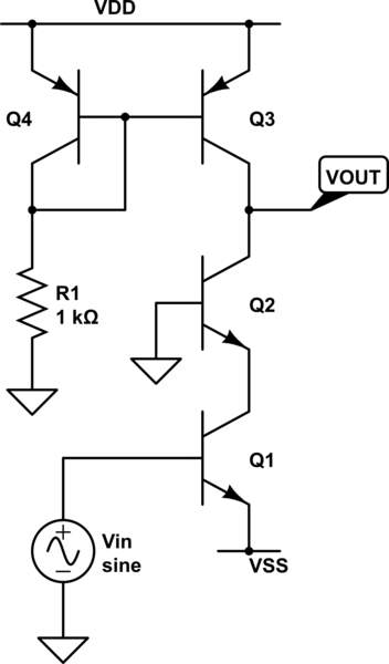
Thermal Noise is big problem with resistors because as resistance or temperature increases, so does the noise. Since nearly everything we, as designers, have to work with has some form of real resistance, we need to deal with thermal noise. Shot Noise, also known as Schottky Noise, primarily exists wherever there is a change in energy levels (such as a PN junction). Thus, if we’re looking at analog circuit, we’ll see it in our friendly BJT. 1/f noise is exactly what the name suggests: noise that varies as the inverse of frequency (to some constant; essentially $\frac{1}{f^{\alpha}}$). We’re going to ignore 1/f noise for now. So first, let’s start off with a BJT Cascode circuit, shown below. Everyone who has been through a basic electronics course has seen this guy and probably analysed the heck out of it. It’s a comfortable circuit. Let’s make it uncomfortable. First, we need some parameters. These are unrealistic and have been chosen to kind of exaggerate the effect of different noise mechanisms in the circuit.
++ I_{C} = 1.8 mA \ \beta_{NPN} = 250 \ \beta_{PNP} = 100 \ f_{t_{NPN}} = 500 MHz \ f_{t_{PNP}} = 250 MHz \ C_{\mu} = 1pF \ R_{BB}’ = 1 k\Omega \ 4kT = 1.66\times 10^{-20} \hspace{5 pt} @ \hspace{5 pt} 27^{\circ}C \ V_{A_{NPN}} = 150 V \ V_{A_{PNP}} = 50 V \ ++
Now that we have the transistor parameters, let’s calculate the gain and bandwidth (we’re going to need both for the noise analysis). Let’s start with the gain. In a cascode, all of your gain is generated by the common-base transistor (the reason this is attractive is that it allows the circuit to have a larger bandwidth than, say, just a common-emitter amp. The reason is because in a common-emitter you have a miller capacitance due to $C_{\mu}$which can be quite large. This causes the dominant pole to be pulled to a lower frequency which, in turn, decreases bandwidth). As such, the gain can be given as the following expression:
++A_{V} = -g_{m}R_{Leq} = -g_{m2}(r_{o2}|r_{o3})++
We know
++g_{m} = \frac{I_{E}}{\frac{kT}{q}}++
and that
++r_{o} = \frac{V_{A}+V_{CE}}{I_{C}} \approx \frac{V_{A}}{I_{C}}++
Since we’re operating at room temperature, $\frac{kT}{q} = 0.0259 V$ so the calculated values are as follows:
- $ g_{m1} = g_{m2} = 69.5 m\mho $
- $ r_{E1} = r_{E2} = 14.4 \Omega $
- $ r_{o1} = r_{o2} = 83.3 k\Omega $
- $ r_{o3} = 27.7 k\Omega $
- $ R_{Leq} = \frac{r_{o2}\cdot r_{o3}}{r_{o2} + r_{o3}} = 20.4 k\Omega $
- $ A_{V} \approx -1400 \ C_{T} = C_{\mu 2} + C_{\mu 3} = 2 pF $
- $ BW = \frac{1}{2\pi R_{Leq} C_{T}} = 3.9 MHz $
Well that was easy, right? Now let’s come up with a noise-equivalent circuit. All that means is that basically we take our normal small-signal model (low frequency model here: we’re ignoring the capacitors) and add in the noise sources. Wherever there is a physical resistance (not equivalent) we need a thermal noise source and wherever there is a pn-junction we need a shot noise source. When all is said and done, there is a total of nine noise sources that need to be evaluated - and all for a simple, 4-transistor cascode amp! The noise equivalent circuit is shown below.
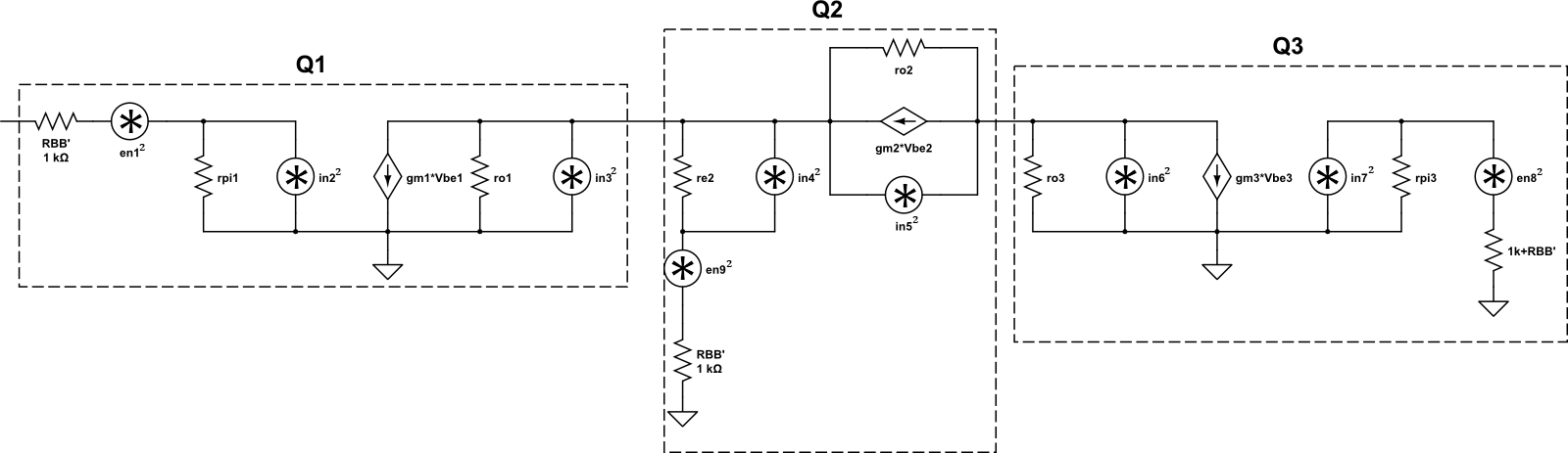
The best approach to analysis the input-referred noise is to first assume that all the noise sources are statistically independent so that we can add them via superposition. The next step is to calculate the noise contribution at the output of the amplifier due to each source, sum them up, and then divide by the square of the gain. So let’s do that!
1) Contribution due to $R_{BB,1}’$.
Since this is thermal noise, the calculation is $ e_{n}^{2} = 4kTR\delta f$ where $\delta f$ is just the bandwidth we calculated earlier. This results in $ e_{n1}^{2} = 6.47\times 10^{-11} V^{2} $. In order to get the noise contribution at the output, this value needs to be multiplied by the square of the gain so that:
++e_{n1,o}^{2} = 6.47\times 10^{-11} (1400)^{2} = 1.27\times 10^{-4} V^{2} ++
2) Contribution due to Base-Emitter PN-Junction in Q1.
Since this is shot noise, the calculation is $ i_{n}^{2} = 2qI_{B}\delta f$. To get $ I_{B}$ we just need to divide the known collector current by $\beta_{NPN}$ so $ I_{B} = \frac{1.8 mA}{250} = 7.2 \mu A$. This results in $ i_{n2}^{2} = 8.99\times 10^{-18} A^{2} $. This needs to be converted into a noise voltage, so we need to determine what resistance this current source sees by setting all other sources to zero. In doing so, it should be fairly obvious that it is just $ r_{\pi 1} | R_{BB}’$. Where $ r_{\pi} $ is just $ r_{E}(1+\beta) = 3.6 k\Omega $. In parallel with $ R_{BB}’$ the current noise source sees $ 783 \Omega $, thus
++ e_{n2}^{2} = 8.99\times 10^{-18}(783)^{2} = 5.51 \times 10^{-12} V^{2}++
Not done yet.
Just like in the first noise source, this one is being ‘gained-up’ by the system on its path to the output, so we need to account for that. As such:
++ e_{n2,o}^{2} = 5.51\times 10^{-12}(1400)^{2} = 1.08\times 10^{-5} V^{2}++
3) Contribution due to Collector-Emitter energy bands in Q1.
Again, this is shot noise so $ i_{n}^{2} = 2qI_{C}\delta f$ which means $ i_{n3}^2 = 2.25\times 10^{-15} A^{2}$. Since we have a current source, we will need to multiply by a resistance to get a noise voltage (as was the case in the last source). By inspection, it’s clear that this resistance will be $ r_{o1} | (r_{E2} + R_{BB,2}’) = 83.3 k\Omega | (14.4 \Omega + 1 k\Omega) \approx 1 k\Omega $. Thus, $ e_{n3}^{2} = 2.25\times 10^{-15}(1\times 10^{3})^{2} = 2.25 \times 10^{-9} V^{2}$. Finally, to get the noise at the output we multiply by the square of the gain, so: $ e_{n3,o}^2 = 4.41 \times 10^{-3} V^{2}$
4) Contribution due to Base-Emitter PN-Junction in Q2.
It should be pretty obvious that this noise source will be negligible, but let’s go on with the calculation anyways. Again, we have shot noise so $ i_{n4}^{2} = 2qI_{B}\delta f = 8.99\times 10^{-18} A^{2}$. The resistance it sees is $ r_{E2}$ so it follows that $ e_{n4}^{2} = 8.99\times 10^{-18}(14.4)^{2} = 1.86 \times 10^{-15}$ which at the output results in: $ e_{n4,o}^{2} = 3.65 \times 10^{-9} V^{2}$ which is roughly ten-thousand times smaller than out previous smallest values . So yes, it’s definitely going to be negligible!
5) Contribution due to Collector-Emitter energy bands in Q2.
Shot noise so $ i_{n}^{2} = 2qI_{C}\delta f$ which means $ i_{n5}^2 = 2.25\times 10^{-15} A^{2}$. The resistance this source sees is just $ r_{o2}$ so $ e_{n5}^2 = 2.25\times 10^{-15}(83.3\times 10^{3})^{2} = 1.56 \times 10^{-5}$. Since this noise voltage is already at the output of the amplifier (the collector of Q2) we _ do not _ need to multiply by the square of the gain. Therefore: $ e_{n5,o}^{2} = e_{n5,o}^{2} = 1.56\times 10^{-5}$
6) Contribution due to Collector-Emitter energy bands in Q3.
Surprise, surprise, we’ve got shot noise yet again. The current noise will be the same as both (5) and (3) where $ i_{n6}^{2} = 2.25\times 10^{-15} A^{2}$. This is where it’s easy to get tripped up. Of course you see the resistance of $ r_{o3}$ but you will also see $ r_{o2} + r_{E2} + R_{BB,2}’ \approx r_{o2}$. Since this ensuing noise voltage is already at the output, no need to multiply by the square of the gain so: $ e_{n6,o}^{2} = e_{n6}^{2} = 2.25\times 10^{-15}(83.3\times 10^{3} | 27.7\times 10^{3})^{2} = 9.36\times 10^{-7} V^{2}$
7) Contribution due to Base-Emitter PN-junction in Q3.
Since this is a PNP we need to calculate $ I_{B}$ which is just going to be $ I_{B,3} = 18 \mu A$. Thus, $ i_{n7}^{2} = 2.25\times 10^{-17}$. Here we see $ r_{\pi 3} | (1 k\Omega + R_{BB,3})’ $ so $ e_{n7}^{2} = 2.25\times 10^{-17}(1.45\times 10^{3} | 2\times 10^{3})^{2} = 1.59\times 10^{-11}$. Now, probably against your intuition, we need to multiply this by the gain of the amp. Well, that’s not exactly true. You see, what’s actually happening is that the noise on the base of Q3 (which is where $i_{n7}^{2}$ is located) is being multiplied by the gain of Q3. If you were to calculate the gain of Q3, you’d see that it is identical to the gain of the system because it has the same transconductance and the same output resistance. But wait: if this is basically just acting as a common-emitter amplifier, shouldn’t the bandwidth of the noise change? YES. The new bandwidth (at least for any noise on the base of Q3) will end up being lowered due to the Miller Effect for $ C_{\mu}$ where the new capacitance is $C_{T,new} \approx C_{\mu}\cdot A_{v} = 1.4 nF $. This yields a new bandwidth of $ 5.6 kHz$ which, in turn, decreases the noise terms to $ i_{n7}^{2} = 3.23\times 10^{-20}$ and $ e_{n7}^{2} = 2.28 \times 10^(-14)$. Thus: $ e_{n7,o}^{2} = 4.47 \times 10^{-8} V^{2}$
8) Contribution due to $ R_{BB,3}’$ and the $ 1 k\Omega $ resistor on the base of Q3.
This is actually the sum of both thermal noise terms for each resistor. Remember that the bandwidth here is not the bandwidth of the amp from input to output but, rather, from the base of Q3 to the output. Thus, $ e_{n8}^{2} = 4kT(1k\Omega + R_{BB,3}’)\delta f = 1.86 \times 10^{-13}$. Multiplying by the square of the gain and we get: $ e_{n8,o}^{2} = 3.64\times 10^{-7} V^{2}$
9) Contribution due to $ R_{BB,2}’$.
This is identical to (1), so: $ e_{n9,o}^{2} = 1.27 \times 10^{-4} V^{2} $
… Phew. Ok, now that we have all the noise terms at the output, let’s sum ‘em up! $ e_{no,total}^{2} = 4.69 \times 10^{-3} V^{2}$ Since we want input-referred noise, however, we just need to divide that value by the square of the gain: $ e_{ni}^{2} = \frac{4.69\times 10^{-3}}{1400^{2}} = 2.39\times 10^-9 V^{2}$ Typically, noise is given in units of $ \frac{V}{\sqrt{Hz}}$ so just divide by the bandwidth and take the square root of the whole thing to get: $ e_{ni} = 24.8 \frac{nV}{\sqrt{Hz}}$ As you can see, the term that has the biggest impact on the circuit noise is clearly due to the collector-emitter path on the input transistor. This is actually analogous to any opamp: the input will cause the most noise (which should make sense because it is ‘gained-up’ by the system). If you were to analyze this circuit again, you could save a significant amount of time by ignoring everything but the shot-noise on the signal-path in Q1 which was $ 4.41 \times 10^{-3}$. Doing so will give you $ e_{ni} = 24 \frac{nV}{\sqrt{Hz}}$ which only differs from the more exact solution by only 3.2% despite ignoring the other eight noise sources. Yeah, I like that approach better too!