Current Steering DAC
For a recent class, our project was to design a 7-bit 5MSPS Current-Steering DAC in 0.5um technology. While the specifications aren’t neccesarily hard to meet, the time-table was rough. We had to go from a pencil-and-paper design to a full physical layout that passed LVS and DRC within about 8 weeks. Yikes. The result, however, would be that the 6 best designs would be selected for fabrication through MOSIS and the chips would arrive sometime in the following two months. Mine happened to be one of the lucky 6! My final paper can be viewed here and will be more comprehensive than this post. Here I’m going to take mainly about hurdles I had to overcome with the design and things I would do differently if I had the chance to take this class again.
The Opamp
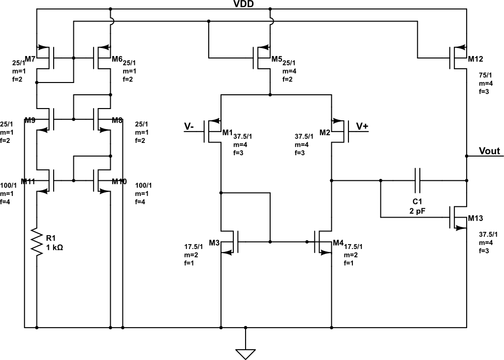
I figure it’s best to start with the heart of the whole operation: the opamp. This little block is responsible for generating a reference current that will be sent out to all of the individual current steering cells. It’s pretty clear that having a pristine reference is massively important, so ignoring this design or not spending too much time on it is not very wise. And this is where I ran into my first problem: I didn’t spend too much time on it (initially, at least). My original design had a gain that varied between 35db and 42db over process, voltage and temperature corners. This was a bit low, but I ran a transient analysis (with a step input on the ‘plus’ pin) and my reference current was stable and only varied by about 0.1 LSB full scale so I figured it would be alright. However, there were a couple issues with my design. First, I didn’t take into account that because the simulations are ideal, I have no systemic offset in my diffpair which is obviously not going to happen in a real layout. Secondly, I forgot about parasitics that will inevitably decrease the amp performance once laid out. I reasoned (key word: reasoned, not calculated) that I was on the very low edge of required system gain and that I should probably look into redesigning the amp. Now was time for some calculations rather than guesswork. You can read how I calculated everything in my paper, but suffice to say that my minimum required gain should be closer to 60dB. Whoops. I would’ve saved a significant amount of time had I done that rather simple calculation initially. Live and learn! Anyways, so now I knew what my minimum gain was so I could set about designing the amp. The architecture itself was pretty simple: diffpair followed by a common-source. Pretty basic. Now I had to figure out what my bias network would be and here comes my second mistake: I picked a constant-gm bias. Now, I knew that I didn’t have access to an external resistor for this bias network and I knew I would have to resort to using an on-chip resistor. This means low precision (around 30%) and would deem the constant-gm bias network rather useless (since gm will be proportional to the bias resistor). If I’m honest, the driving reason behind choosing this network was that I just wanted to have an on-chip resistor that I could lay out since I hadn’t done that before. Poor reasoning, but there it is. If I was a smart designer, I would have chosen a bias network that utilizes the reference current I’m generating so that it would be self-biasing. But that quick 8-week turnaround was really worrying me, so actually sitting down and figuring out how to self-bias my amp like that was, quite frankly, kind of scary. So I took the dumb-road and went with a constant-gm network. ‘Tsk, tsk’, I know.
The layout was one of the few things I think I did right from the very beginning (which was pretty remarkable for it being my first true physical layout). I was able to get everything to be very compact, I made sure to interdigitate the diff-pair and lay them out in a common-centroid pattern (to help with matching), and I laid my 2pF capacitor out using multiple smaller sections in parallel rather than one big blob of poly. This is probably the only block layout I really wouldn’t do much different with other than adding a guard-ring (something I overlooked on all of my blocks though).
The Decoder
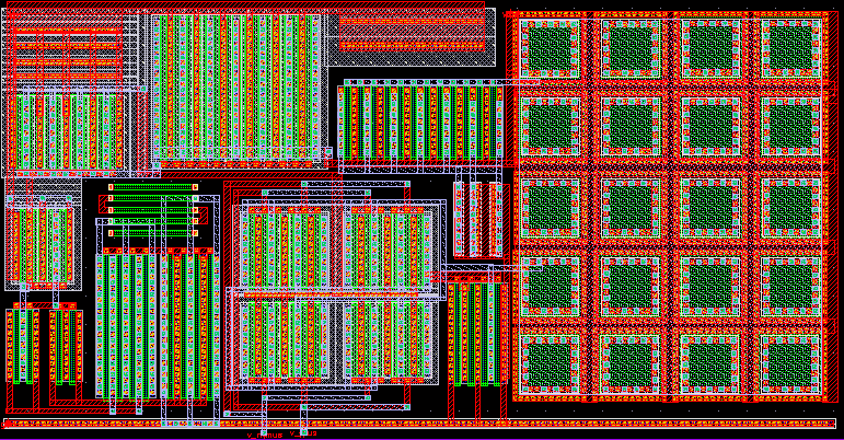
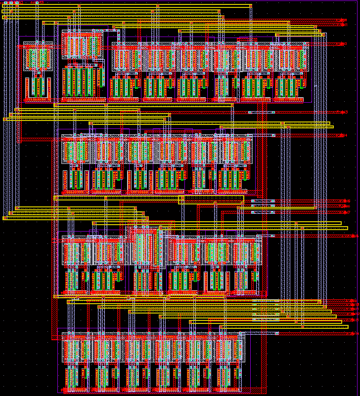
The next important block is the decoder. Here thermometer logic was used due to its intrinsic monotonicity. Since the design is only 7-bits, creating this decoder wasn’t very difficult: essentially I just had to create a truth table and then implement that function. I split the decoders into a 3-bit decoder (row) and 4-bit decoder (column) to simplify the logic. I didn’t use a NAND or NOR only implementation and ended up using a variety of AND and OR gates. If I wanted my design to be more efficient (and to cut down on gate-delays) it would’ve made sense to use only NAND or NOR gates. I wasn’t too worried about these issues, however, so I stuck with the ‘lazy’ implementation. A bit of an oversight was that my transistor sizing wasn’t very smart. Instead of using a fanout approach (where I minimize delays by sizing a transistor based on what it’s driving), I sized everything to one unit resistance (which I arbitrarily picked- you can read that in the paper). The layout is where everything went awry. My row decoder (not shown) wasn’t awful, though. My strategy, just to simplify the layout process for myself, was to organize blocks into equally sized rows and have all the outputs located at the top of the cell. This was a decent approach, though there was a good amount of unused space, unfortunately. The column decoder was a bit larger and my row-decode strategy did not end up translating very well. As you can see in the figure, there is a ton of unused space - way more than I would’ve liked. By the time I realized just how much unused space there would be, however, I was already knee deep in the layout and had no time to re-do it. I’m really upset with the way it turned out and I’m just lucky that the layout of the decoder wasn’t critical for proper operation (like the opamp and current cell layouts are).
The Current Cell
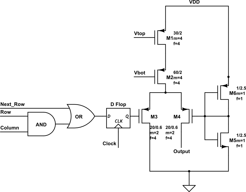
The last real critical block was the current-cell. Now one design choice I made that I later regretted was not stepping down the local logic supply from 5V to something lower like 3V. The reason I decided not to drop the level was that I’d have to put more time into sizing the current switches to guarantee only one is conducting in either state (on/off). Again, that 8-week timetable was pretty scary - especially with a plethora of other things on my plate. The benefits of lowering the voltage would’ve been worth it though as my settling time would’ve massively decreased. Another oversight was that I sized my CMOS divider a bit too large and end up conducting 20uA (which results in a fairly large amount of power when multiplied by 127 cells). Realistically I could’ve brought that current draw down much, much lower and really don’t know why I didn’t just take the 2 minutes to change the sizes. Definitely an oversight.
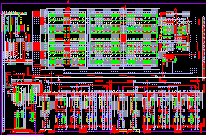
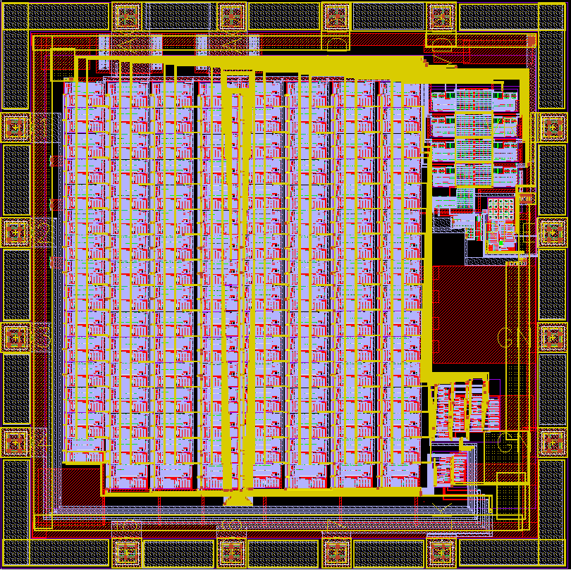
Now the layout is… okay. I’m decently happy with how compact I got it (there is certainly room for improvement) but something quite unfortunate happened which resulted in my doing something incredibly dumb: I forgot I had a size constraint. When I went to lay out all 127 cells, I did not fit within my pad ring (1.3 mm x 1.3 mm). I had to remake the layout (which is shown above) to make it more rectangular and in my panic-stricken state ended up placing the ports such that some digital lines would be forced to cross over some analog portions of each cell. Routing all that digital noise near what should be a really clean analog line is bad, bad, bad. It’s one of those things, though, where I’m glad I made this mistake because it’s one I will remember to NEVER make again. Black clouds, silver linings, etc. To try and mitigate this, I made sure to surround my analog output line in grounded metal (sides, top and bottom) to try and keep it as clean as possible up until the points where the digital lines come in to ruin the day. The final layout is shown below and I’ll be adding to this post once the chip comes in from the fab. Hopefully everything works great!
- Share this post!


