Circuit Design Interview Questions: Part III
Building off of my previous posts Circuit Design Interview Questions: Part I and Part II, we’ll now explore the last set of questions that require some decent knowledge of frequency response characteristics of amplifiers and MOSFETs.
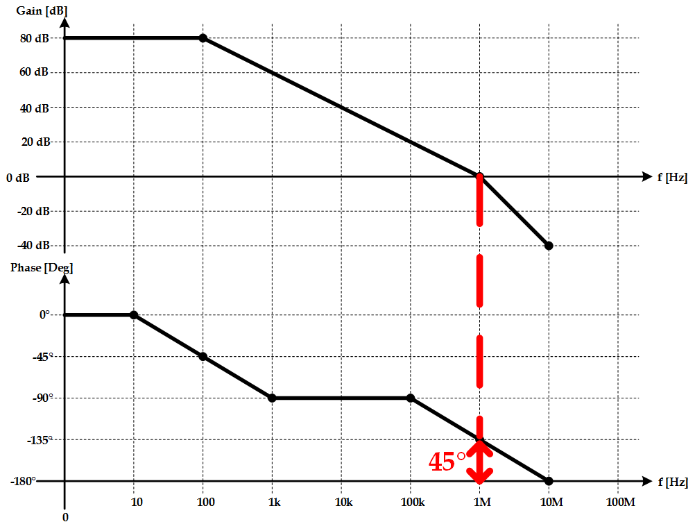
Question 9
Sketch the bode plot of a two-pole inverting amplifier with DC-gain of 80 dB, GBW of 1 MHz, and a phase margin of 45 degrees.
Solution
This question is nice as it requires knowledge of how the gain and phase behaves at different frequencies given pole locations. Given our known variables, we know that the gain of the amplifier will be 0 dB at 1 MHz. We also know that the phase should be 45 degrees at 1 Mhz because that is our given phase margin. First, however, let’s deal with the gain plot. We know that there must only be one pole before the 0-dB crossing since our phase margin has shifted less than 180 degrees (as evidences by the positive phase margin value). Thus, the gain will decrease by 20 dB per decade from the first pole location (which we still have to find) to the 0-db crossing (and possibly beyond). As the bode plot below shows, we hit 80 dB at 100 Hz and, since this is our DC-gain, the gain “clamps” and flat-lines out to 0 Hz. Clearly, we have our first pole at 100 Hz. Now let’s take a look at the phase. We know that between one decade before and one decade after a pole frequency, the phase will have shifted by 90 degrees. Thus, at a given pole frequency the phase will be shifted by 45 degrees. This then implies that the phase should be -90 degrees at 1 kHz, as shown in the bode plot. Now we know there is one more pole, as given by the problem statement. We also know that the phase MUST shift by another 45 degrees and that this value MUST be located at 1 MHz. This implies that the second pole is actually at 1 MHz and the phase will shift to -180 degrees at 10 Mhz. As a further addition to the graph, the gain can also be extrapolated to 10 Mhz. Since a second pole has been encountered, the gain will begin to shift by 40 dB per decade (as opposed to 20 dB per decade). The plot of all this is shown below:
Question 10
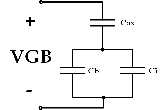
Sketch the small-signal model for a MOS capacitor.
Solution
This can easily be accomplished with an understanding of the causes of capacitance within a MOSFET. Obviously, there is the oxide capacitance but there are also two other capacitances caused by the depletion layer, $ C_{b} $ and by the inversion layer, $ C_{i} $. This equivalent circuit, therefore, is shown below.
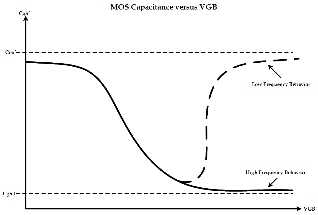
Question 11
Given a MOS Capacitor, sketch the capacitance vs. voltage curve at both low frequency (<1Hz) and high frequency (>100kHz).
Solution
I love MOSFETs and capacitance-based questions are great as they’re some of the first things you’re exposed to in an advanced FET class (since they’re just a two-terminal device). A plot of this capacitance is shown below. The capacitance at low values of VGB are approximately equal to the oxide-capacitance (although, recalling the previous question, cannot be exactly equal since the parallel combination of the inversion and depletion capacitors are in series with the oxide capacitor). At low frequencies, the inversion charge is able to change at the same rate as VGB and, thus, the inversion layer capacitance is larger at increasing values of VGB (remember, Q=VC). However, since the concentration of electrons can only be changed by thermal generation and recombination, the inversion charge struggles to keep up with a rapidly changing VGB. This results in a smaller amount of inversion charge which decreases the overall MOS capacitance.
(As a note: my absolute favorite textbook is called “Operation and Modeling of the MOS Transistor” by Yannis Tsividis and Colin McAndrew. Anybody with an interest in MOSFETs should absolutely BUY THIS BOOK as it explains everything you’d ever want to know about MOSFETs in a really great and understandable way.)