Circuit Design Interview Questions: Part I
We recently had a few co-ops come in for interviews and two of the guys I worked with needed to come up with some questions to ask. Neither them nor I had any experience on the other side of the table (in that we’ve never given interviews before) so we started talking about questions we’ve been asked in other interviews. I wrote down a bunch of good ones we talked about and decided to share them! The whole goal is to just test their ability to think through a problem so I tried to write down ones that had a mix of that as well as some fundamental theory any EE grad should know.
Question 1
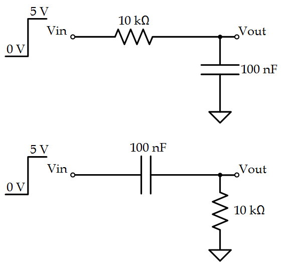
Draw the voltage at the node $ V_O $ for the following circuits.
Solution
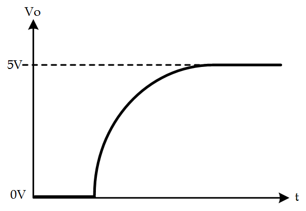
I like this question a lot because it’s simple and should be easily solvable by any student with at least some circuit theory exposure. The first circuit is simply a low-pass-filter. When the step is applied, the changing voltage causes the capacitor to charge up to the input voltage until $ V_O = V_{in} $. A plot of the output voltage is shown below:
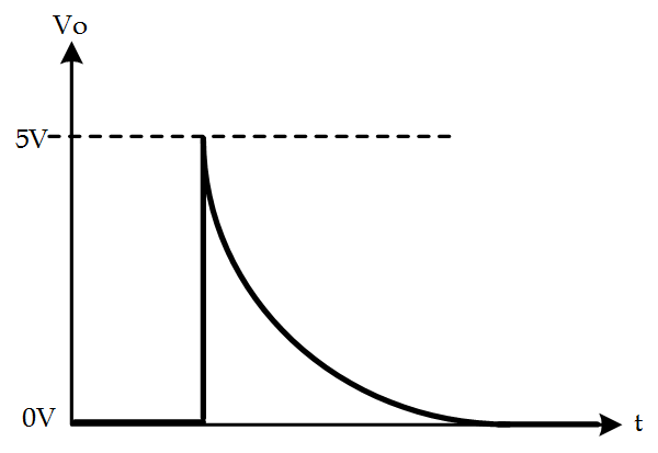
The second circuit is a high-pass-filter. Here, the quickly changing input voltage is allowed to pass through the capacitor which causes $ V_O $ to be shorted to $ V_{in} $. When the step on the input settles to it’s final DC voltage of $ 5\,V $, the capacitor blocks the input and the voltage on the $ V_O $ node is bled through the resistor until it settles to $ 0\,V$. A plot of the output voltage is shown below:
Question 2
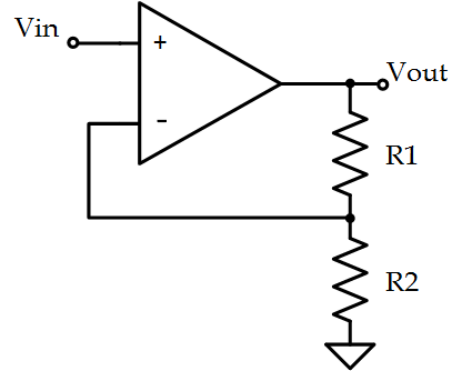
What is the closed-loop DC-gain of the following circuit?
Solution
This is a nice question because it tests a student’s understanding on basic Op Amp analysis. Since the voltage on the inverting and non-inverting terminals are equal, KCL can be used to find $ \frac{V_O}{V_{in}} $. Since $ \frac{V_{in}}{R_2} = \frac{V_O-V_{in}}{R_1} $ it’s clear that the voltage gain is: $ \frac{V_O}{V_{in}} = 1+\frac{R_1}{R_2} $ Very basic, and definitely a fair question to ask in any interview.
Question 3
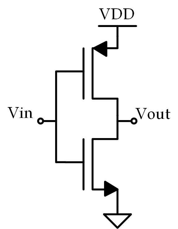
What is the small-signal gain of the following circuit? (Assume $ \lambda_N = \lambda_P $)
Solution
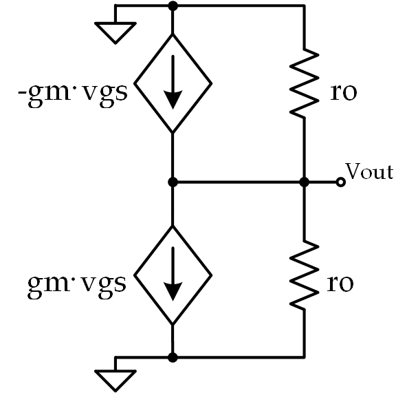
Out of the ten questions in this whole series, this is probably my favorite because nearly every engineer you run in to will immediately think “That’s an inverter!” (which it is) and balk a bit when you ask for the small-signal gain. It’s a familiar circuit used in a somewhat unfamiliar context which is why I think it’s great. So what’s the solution? It’s essentially just a common-source amplifier but don’t take my word for it: let’s look at the small-signal model:
Using KCL we see that $ 2g_mv_{in} + \frac{2v_o}{r_o} = 0 $ Which, in turn, implies: $ \frac{v_o}{v_{in}} = -g_mr_o $ Which is the same as a common-source amplifier. Of course, small-signal analysis isn’t necessary to solve this problem, but it helps illustrate where the solution comes from.
Question 4
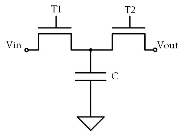
What is the equivalent resistance of the following circuit assuming that $ T_1 $ and $ T_2 $ are switched alternately at a frequency $ f_s $? (Assume ideal MOSFETs)
Solution
Now I like this because it helps to illustrate an interviewee’s thought process. It’s simply a switched capacitor, but if you have never been exposed to them previously it definitely makes you think a bit. I think the best approach is just to think about what happens at the node of the capacitor as each FET is switched. For the duration of $ T_1 $, the capacitor will begin to charge to the voltage at $ V_{in}$. This voltage will then be seen at $ V_O $ during the time $ T_2 $ so the main event is the charging during $ T_1$. Well, we know the equation for charge on a capacitor is: $ Q = VC $ We also know that a Coulomb (a single unit of charge) is equivalent to an Ampere-second so: $ I\cdot t = VC \ \frac{I}{f_s} = VC $ From here just solve for the equivalent resistance, $ \frac{V}{I} $, which ends up being $ R_{eq} = \frac{1}{Cf_s} $. Stay tuned for Part II (UPDATE: Part II Here)!
