4-bit CPU
For a Computer Architecture class last year each student was tasked with designing a CPU with a given set of specifications. My specs were:
- Indexed Memory Address Arithmetic
- Multiplexers (as opposed to tri-state buffers)
- Two bus design
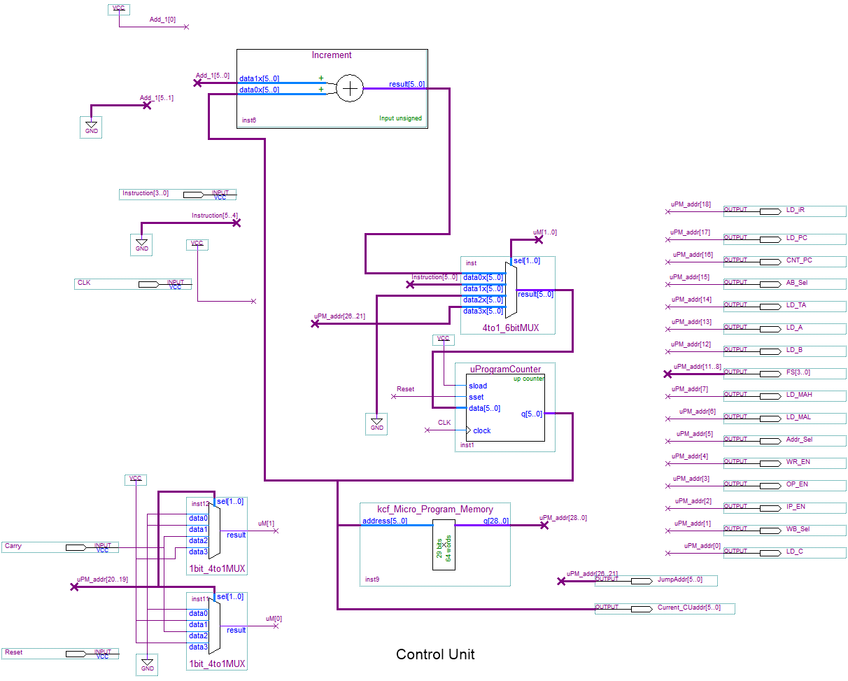
- μProgrammed control unit
- I/O mapped peripherals
- Von Neumann architecture
Every student had at least one spec that differed so it guaranteed that each design was different (even though a chunk may be quite similar). It was definitely a good experience and the outcome was pretty neat too! Unfortunately, I didn’t have the presence of mind to take pictures of the hardware implementation (the designs were uploaded to Altera FPGAs) so all I have are my design simulations. Below is my full write-up with reference pictures. Hopefully it’s informative! As a note, the software used was Altera Quartus II 10.1.
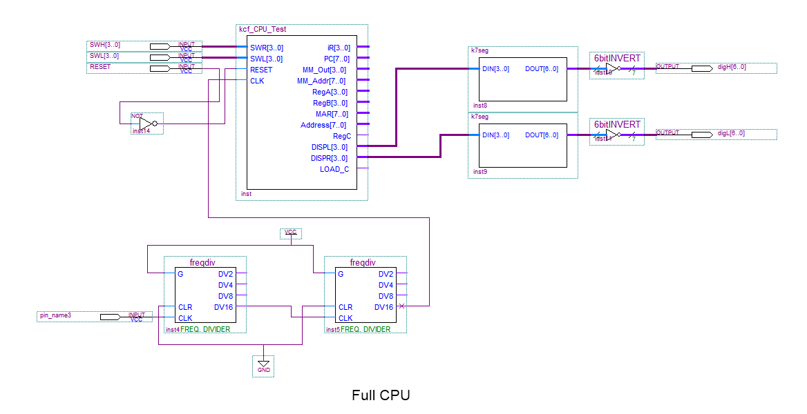

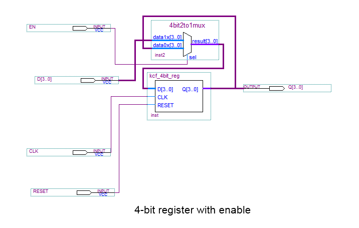
The processor had to be designed with functionality for addition, subtraction, increment, decrement, logic and, logic or, logic not, logic xor, jump conditional, jump unconditional, write, read, swap and copy instructions as well as the ability to receive an input from switches and write an output to seven segment displays. There were two four bit registers required in the final design with eight bit wide memory addresses used for program and data memory.
The first design specification was that of Indexed Memory Address Arithmetic. In the data-path of the processor, the effective Memory Address is computed by simply taking the high Memory Address and concatenating it with the low Memory Address when the most significant bit, MAH7, is 0. However, when that value goes to 1, the effective Memory Address becomes 0x0 concatenated with the contents of register B. This was implemented by simply feeding 0x00 into the data0 line of an 8-bit 2 to 1 multiplexer and 0x0 concatenated with the contents of register B fed into the data1 line of the same multiplexer. The select sign of the mux is controlled by the MSB of MAH. The mux’s output is then fed into an 8-bit adder with the other signal into the adder being the effective memory address. This setup was chosen due to the fact that the effective memory address would always be itself unless the MSB is a 1, in which case 0x0 will be concatenated with B and added to the MAeff.
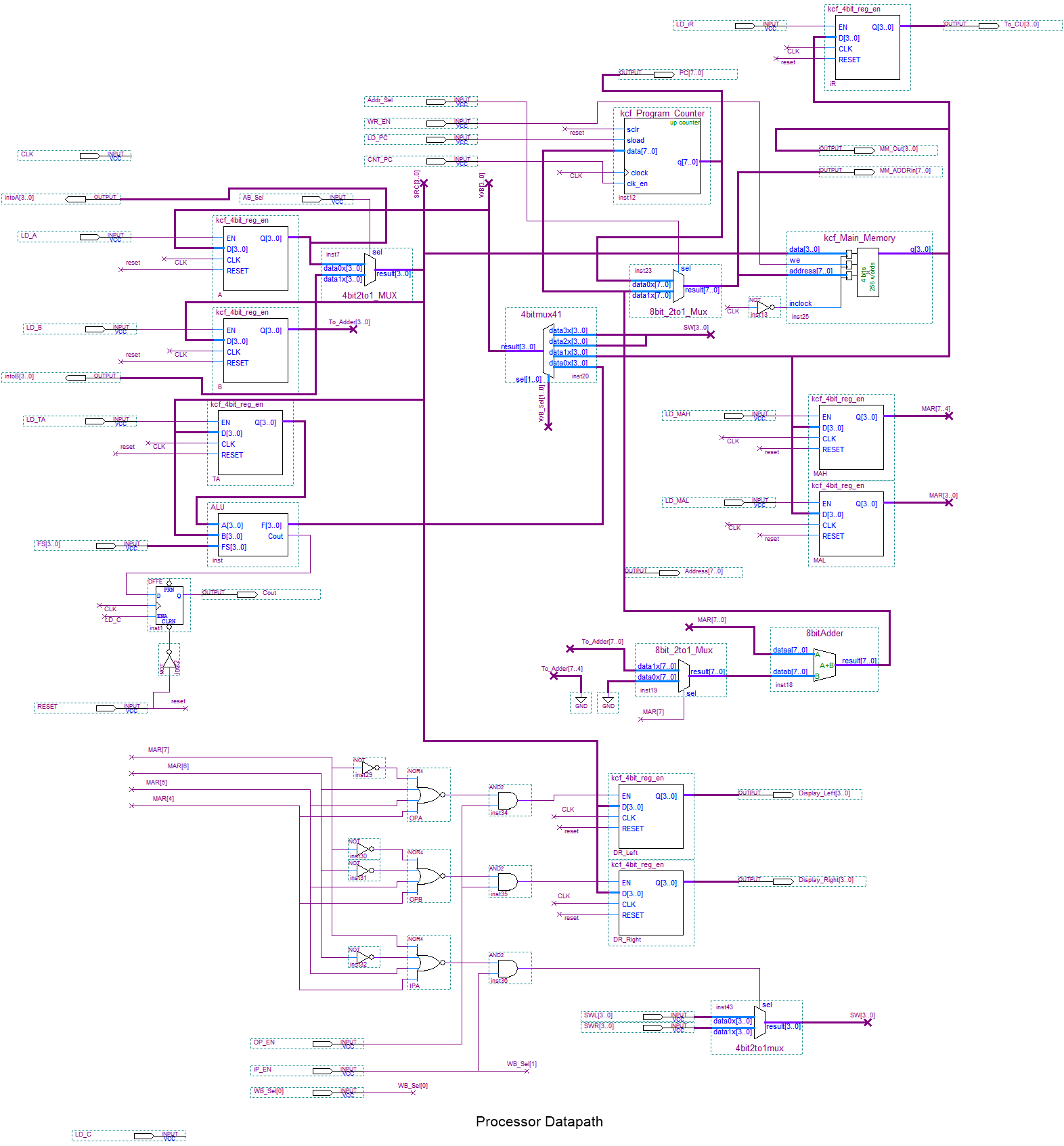
The next design specification was to implement multiplexers rather than tri-states. This is a fairly self-explanatory design parameter in that every signal that needs to be enabled is controlled by the select signal on a multiplexer rather than each bus having an enable switch, which would be dictated by tri-states. In order to transfer data, two busses were required in this specific processor design. In order to efficiently transfer data a third bus would have been ideally included but as this design only required two, some measures had to be taken in place so as not to cause any timing errors with instructions. This causes delay with the processor but as it is only a 4-bit CPU, the delay is negligible. The instructions are controlled by a micro-programmed control unit which is essentially a block of memory controlled by multiplexers which is initialized with the instructions to be implemented. The muxes control which memory address to go to fetch an instruction and immediately after an instruction is fetched; it produces a total of eighteen control signals which control the workings of the datapath.
A further design specification was to have I/O mapped peripherals. This required the design of three sets of logic circuits. The first two controlled the enables of output registers which, in turn, controls either the left or right seven segment display. These had to be designed so that when a specific value from memory was output (and the output enable signal from the control unit was HIGH), the logic circuit would relay a HIGH to the needed register. The third logic circuit controls a select signal on a mux which selects between two separate switches. This was designed in a similar fashion to the output logic in that it was designed to output a HIGH during a specific memory value. The final specification was that the CPU had to be of a Von Neumann architecture. This requires the use of a single initialized Main Memory block which contains both the program and data memory (as opposed to two separate memory block for program and data). The design choices were fairly simple and functioned well with only few errors occurring on the final compilation, all of each which were easily remedied. The datapath design required more thought that originally planned due to the Von Neumann and Multiplexer requirements. In order to write any data values back to the internal busses, a four-bit four-to-one mux had to be used. The select signal for this component was generated by two signals. The first was called WB_Sel and controlled the LSB of the select. The other was iP_EN, which controls input peripherals, and controlled the MSB of the select. Because of this design choice, the output of the input peripherals had to be wired into the data2 and data3 slots of the multiplexer so that only when iP_EN was high would it select the switches. This initially seems redundant as the input peripherals are controlled by that signal to begin with via the control logic, which will be discussed later, but is a requirement as, in the mux, its purpose is more to control when the switches should not write onto the internal busses.
In order to write values from the ALU, the output had to be wired into this multiplexer as well. However, two data lines were still open with only one more signal needing to be wired in, and that would be the output of the Main Memory block. I chose to wire the ALU to data0 as then the control unit would not have to generate any signal to tell the ALU to write back to the internal busses and all the control unit would effectively need to determine when the ALU does not need to write back. This seemed to be an efficient solution, though with a CPU this small the potential benefits would not be able to be fully realized. The final specific design choice that needed to be implemented for my particular CPU was the addition of an inverter on the clock input on the Main Memory block. This is due to the inherent timing issues associated with the Von Neumann architecture and is a simple solution that guarantees memory will be read from or written to during the correct clock cycle. The control unit design was very simple and almost elegant when compared to the datapath (strictly due to the amount of components involved in each). The control unit, being micro-programmed, contained an initialized ROM block with a six bit address width and 28 bit data out bus width. The output on the ROM controls signals within the control unit itself as well as signals in the datapath. A four-to-one multiplexer was used to control where in the micro-programmed memory the control unit would need to jump (for example, going from instruction ADD1 to ADD2 and then back to instruction fetch). This was done quite simply by building an increment block and by tying six bits from the data out on the ROM to the mux. The six bits would correspond to a six bit jump address in memory which, incidentally, would be initialized in memory. The increment block allowed for multiple instructions to be placed consecutively in memory, allowing the control unit to just follow an instruction sequentially.
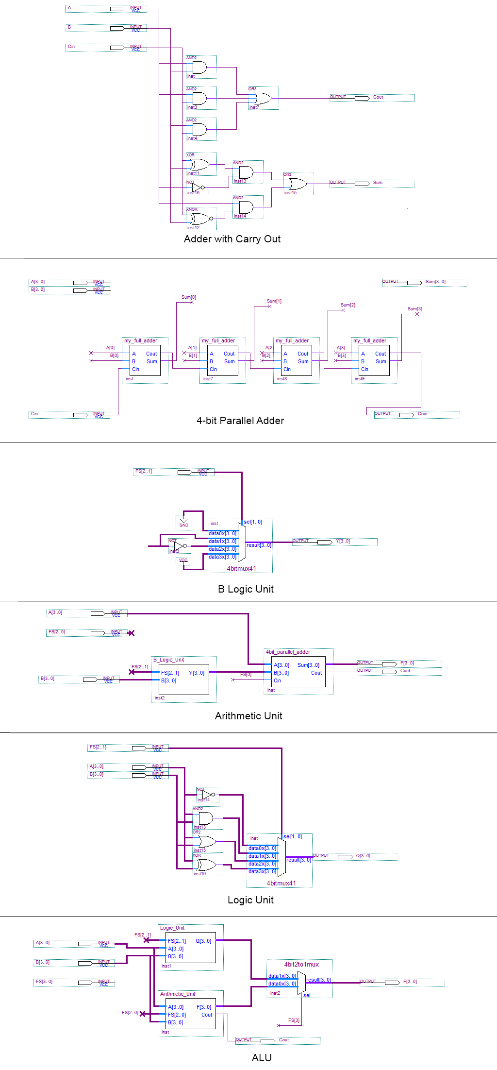
The benefit here is more for debugging purposes as it is clearer to the designer what the control unit is actually doing. A third data line to the mux was tied to a busline coming from the datapath which would determine what instruction should be executed. Since the instructions in this design were only four-bits and the memory in the control unit was six-bits, the first two most significant bits of the instruction were tied to logic LOW so that the first instruction would be “0-0-0-0-0-0”. The choice was made for simplicity when debugging. An important addition in the control unit block was the use of two multiplexers that would determine the conditional statement in the conditional jump instruction. Effectively, the output of these two muxes served as the select signals to the control unit main mux discussed previously. Only on the jump conditional statement was the output of the carry register from the datapath analyzed and otherwise the data lines were set up so that the original mux design would be effectively unchanged. Before I describe the compilation of the datapath and control signal, it is worth mentioning a design choice that took place deep within the CPU. A four-bit adder was one of the first designs used in the CPU and could be implemented very easily with a large array of gates. I opted for XOR and XNOR gates as they have less transistors than the popularly chosen AND gates and would result in faster speeds and less power consumption. Of course, due to the small nature of the CPU these effects were negligible, I still wanted to take those parameters into consideration as in the professional world, they would be ideas well worth considering. (Below is a test of the datapath signal routing)

At the final compilation of the CPU, a few slight changes needed to be made. The first being that two frequency dividers needed to be placed on the clock of the CPU in order to guarantee the CPU would run as intended and to avoid potential timing issues as the FPGA used contains a faster clock than what was used in simulation. The next was that an inverter needed to be placed on the reset signal. For some reason or another, the circuit, when tested on the FPGA, was constantly in reset until the physical reset button was pressed down to logic HIGH. The last tweak was that an inverter needed to be placed on the output of the seven-segment decoders in order to properly display the desired values. Surprisingly, there were no hardware design flaws at the end of the processor build. There were, of course, hiccups, but all of those boiled down to either programming errors or an incorrect bit in the control unit ROM initialization file (which were easily, and quickly, tracked down and rectified). The following is the initiailization file for the μProgrammed Control Unit
-- Control Memory Initialization File

WIDTH = 29;
DEPTH = 64;

ADDRESS RADIX = HEX;
DATA_RADIX = BIN;

CONTENT BEGIN %Control Signal Names%
00 : 00010000110000100000000000000; %ADD1%
01 : 00010001110000100000000000000; %SUB1%
02 : 00010010110000100000000000000; %INC1%
03 : 00010011110000100000000000000; %DEC1%
04 : 00010100110000100000000000000; %NOT1%
05 : 00010101110000100000000000000; %AND1%
06 : 00010110110000100000000000000; %OR1%
07 : 00010111110000100000000000000; %XOR1%
08 : 00011111110010000000010000000; %JMPU1%
09 : 00100001110010000000010000000; %JMPC1%
0A : 00011000110001100000000000000; %SWAP1%
0B : 00111111110000001000000000000; %CPY1%
0C : 00011001110010000000010000000; %WR1%
0D : 00011011110010000000010000000; %RD1%
0E : 00011101110010000000010000000; %IN1%
0F : 00011110110010000000010000000; %OUT1%
10 : 00111111110001010001000000001; %ADD2%
11 : 00111111110001010010100000001; %SUB2%
12 : 00111111110000010000100000001; %INC2%
13 : 00111111110000010011000000001; %DEC2%
14 : 00111111110000010100000000000; %NOT2%
15 : 00111111110001010101000000000; %AND2%
16 : 00111111110001010110000000000; %OR2%
17 : 00111111110001010111000000000; %XOR2%
18 : 00111111110000011000000000000; %SWAP2%
19 : 00000000000010000000001000000; %WR2%
1A : 00111111110000000000000110000; %WR3%
1B : 00011100000010000000001000000; %RD2%
1C : 00111111110000010000000100010; %RD3%
1D : 00111111110000010000000000100; %IN2%
1E : 00111111110000000000000001000; %OUT2%
1F : 00100000000010000000001000000; %JMPU2%
20 : 00111111110110000000000000000; %JMPU3%
21 : 00111111100010000000001000000; %JMPC2%
22 : 00111111110110000000000000000; %JMPC3%
23 : 00000000000000000000000000000; %BLANK%
24 : 00000000000000000000000000000; %BLANK%
25 : 00000000000000000000000000000; %BLANK%
26 : 00000000000000000000000000000; %BLANK%
27 : 00000000000000000000000000000; %BLANK%
28 : 00000000000000000000000000000; %BLANK%
29 : 00000000000000000000000000000; %BLANK%
2A : 00000000000000000000000000000; %BLANK%
2B : 00000000000000000000000000000; %BLANK%
2C : 00000000000000000000000000000; %BLANK%
2D : 00000000000000000000000000000; %BLANK%
2E : 00000000000000000000000000000; %BLANK%
2F : 00000000000000000000000000000; %BLANK%
30 : 00000000000000000000000000000; %BLANK%
31 : 00000000000000000000000000000; %BLANK%
32 : 00000000000000000000000000000; %BLANK%
33 : 00000000000000000000000000000; %BLANK%
34 : 00000000000000000000000000000; %BLANK%
35 : 00000000000000000000000000000; %BLANK%
36 : 00000000000000000000000000000; %BLANK%
37 : 00000000000000000000000000000; %BLANK%
38 : 00000000000000000000000000000; %BLANK%
39 : 00000000000000000000000000000; %BLANK%
3A : 00000000000000000000000000000; %BLANK%
3B : 00000000000000000000000000000; %BLANK%
3C : 00000000000000000000000000000; %BLANK%
3D : 00000000000000000000000000000; %BLANK%
3E : 00000000010000000000000000000; %iF1 0x0040000%
3F : 00111110111010000000000000000; %iF0 0x3EE8000%
END;
The following is a sample program for the CPU that multiplies two numbers together (note there is no multiplication instruction in the instruction set!)
-- Memory File

WIDTH = 4;
DEPTH = 256;

ADDRESS_RADIX = HEX;
DATA_RADIX = HEX;

CONTENT BEGIN
00 : E;
01 : 0;
02 : C;
03 : 6;
04 : F;
05 : B;
06 : 1;
07 : C;
08 : 7;
09 : F;
0A : B;
0B : D;
0C : 6;
0D : F;
0E : 3;
0F : C;
10 : 6;
11 : F;
12 : 9;
13 : 2;
14 : 6;
15 : E;
16 : 4;
17 : 0;
18 : B;
19 : 9;
1A : 0;
1B : B;
1C : D;
1D : 7;
1E : F;
1F : 2;
20 : C;
21 : 7;
22 : F;
23 : 8;
24 : 0;
25 : B;
26 : A;
27 : F;
28 : C;
29 : D;
2A : 7;
2B : F;
2C : F;
2D : 8;
2E : C;
2F : 8;
30 : 0;
31 : 2;
32 : D;
33 : 8;
34 : 0;
35 : 8;
36 : 0;
37 : 0;
END;
- Share this post!


